Active Metal Brazing (AMB) Paste
Product Description
Active metal brazing copper process (AMB) is a method in which a small amount of active elements in the filler metal reacts with the ceramic to form a reaction layer that can be wetted by the liquid filler, thereby bonding the ceramic to the metal.
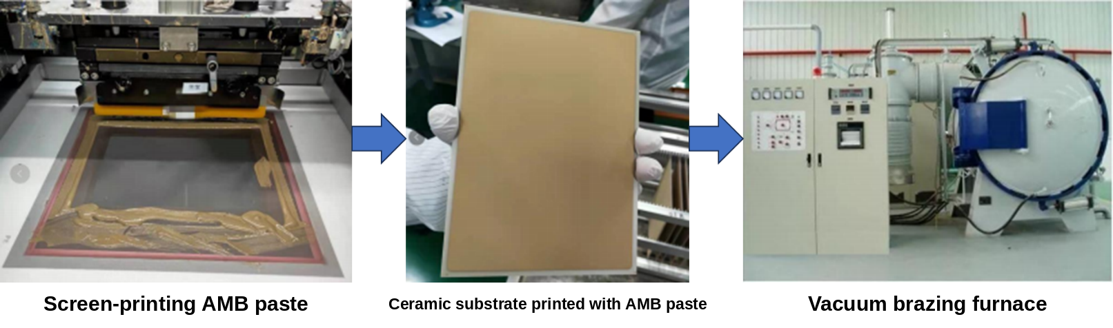
The ceramic surface is first screen-printed with active metal braze paste, then clamped together with oxygen-free copper and brazed at high temperature in a vacuum brazing furnace. After bonding, the substrate undergoes a wet-etching process similar to that used for PCB manufacturing to form circuit patterns on the surface, and finally surface plating is applied to produce a reliable, high-performance product.
AMB substrates achieve bonding through a high-temperature chemical reaction between the ceramic and the active metal braze paste, resulting in higher bond strength and better reliability. However, because this method is costly, suitable filler materials are limited, and the filler has a major impact on bonding reliability, only a few Japanese companies have mastered high-reliability active metal brazing technology.
Through optimization of various filler formulations, we have developed a dedicated active braze paste system for the active brazing of ceramics such as aluminum nitride (AlN), silicon nitride (Si3N4), and aluminum oxide (Al2O3). This paste offers a simple preparation process, excellent printing characteristics, good wettability with ceramics, and high bond strength after brazing.
。

By combining paste screen-printing technology with vacuum brazing technology, excellent bonding between the ceramic substrate and copper is achieved. Through research into sintering methods and ceramic substrate characteristics, we adopted a special formulation design concept that provides excellent control over bond strength and the bonding interface, achieving an interfacial void ratio of less than 0.05%.
Product Specifications
|
Product Name
|
Ag-Cu-Ti Active Metal Paste
|
|
| Application Area | AlN, Al2O3, Si3N4 and other ceramic substrates, for brazing to metals and non-metals | |
| Appearance | Yellow or brown | |
 |
 |
|
| Metal Powder | Silver powder, copper powder, silver alloy powder, copper alloy powder, etc. | |
| Resin | Acrylic resin, PVB resin, ethyl cellulose, etc. | |
| Solid Content | 70-85% | |
|
Viscosity
(25°C, DV2T, 5 rpm)
|
60-120 Pa·s | |
| Recommended Drying Temperature | Forced-air oven or tunnel furnace, 150°C/10 min | |
| Recommended Sintering Temperature |
Under vacuum, 800-900°C
|
|
Product Advantages
|
Property
|
AlN |
Si3N4
|
|||
| Brazing Wettability | ≥99% | ||||
| Brazing Void Ratio | 0.3 mm Cu thickness | ≤0.05% | 0.3 mm Cu thickness | ≤0.05% | |
| - | 0.5/0.8 mm Cu thickness | ≤1% | |||
| Peel Strength | ≥10N/mm | ||||
|
Thermal Cycling (-40~150°C)
|
>3000 cycles | >5000 cycles | |||
| Rapid Thermal Cycling (0~400°C) | >30 cycles | >60 cycles | |||
Note: The data above were obtained under laboratory conditions and are for reference only; actual results should be based on data from customer applications.
Void Ratio After Sintering
|
Scanning image after sintering, before etching
|
||
 |
 |
 |
| Imported Paste A | Ample Paste | Domestic Paste B |
Substrate: AlN, copper foil thickness 0.3 mm
Comparison of void-ratio scan images of three pastes after sintering, ×1000
As shown in the image, our in-house paste has a low void ratio close to 0%, the imported paste has a void ratio of <0.03%, and a certain domestic paste has a void ratio of <0.05%.
|
Scanning image after etching and rapid thermal cycling
|
||
 |
 |
 |
| Imported Paste A | Ample Paste | Domestic Paste B |
Scanning images of the above products after etching and 40 cycles of rapid thermal cycling (0~400°C).
As shown, our in-house paste exhibits stable performance, with no significant increase in void ratio.
 |
 |
 |
| Imported Paste A | Ample Paste | Domestic Paste B |
Above: substrate is silicon nitride, copper thickness 0.8 mm.
In general, the thicker the copper, the more difficult brazing becomes and the higher the void ratio. Our paste employs a special design concept that maximizes high-temperature wettability and leveling, while optimizing for differences in melting viscosity, diffusion coefficient, and CTE among the powder components. As shown in the comparison above, our paste shows a clear advantage in thick-copper applications.
 |
 |
 |
| Imported Paste A | Ample Paste | Domestic Paste B |
Comparison images after copper foil etching and titanium nitride etching.
As shown above, both our Ample paste and the imported paste show no noticeable residue and minimal undercutting after etching, while a certain domestic paste shows clearly incomplete etching and severe undercutting.
| Group | No. | Sample 1 | Sample 2 | Sample 3 | Average | ||||
| Side A | Side B | Side A | Side B | Side A | Side B |
Side A |
Side B | ||
|
Imported Paste A
|
Copper layer
initial separation / cycles
|
78 | 80 | 80 | 80 | 78 | 80 | 78.6 | 80 |
|
Copper layer
clear separation / cycles
|
/ | / | / | / | / | / | / | / | |
|
Ample Paste
|
Copper layer
initial separation / cycles
|
>80 |
>80 |
>80 |
>80 |
>80 |
>80 |
||
|
Copper layer
clear separation / cycles
|
/ | / | / | / | / | / | / | / | |
| Domestic Paste B |
Copper layer
initial separation / cycles
|
60 | 60 | 58 | 60 | 60 | 60 | 59.3 | 60 |
|
Copper layer
clear separation / cycles
|
78 | / | / | / | / | / | / | / | |
Substrate: silicon nitride, copper thickness 0.3 mm, thermal cycling 0~400°C; the value recorded is the cycle at which the copper layer first begins to separate from the ceramic substrate. An entry of ">80" indicates that no separation was observed within the 80-cycle test.
Studies show that the vast majority of power device failures are related to inadequate heat dissipation, making the thermal performance of the ceramic substrate critical to power device reliability. AMB substrate reliability depends heavily on key factors such as the active filler composition, the brazing process, and the microstructure of the brazed layer.
As shown in the table above, our paste demonstrates excellent thermal-shock reliability, outperforming both comparison pastes.
Application Areas
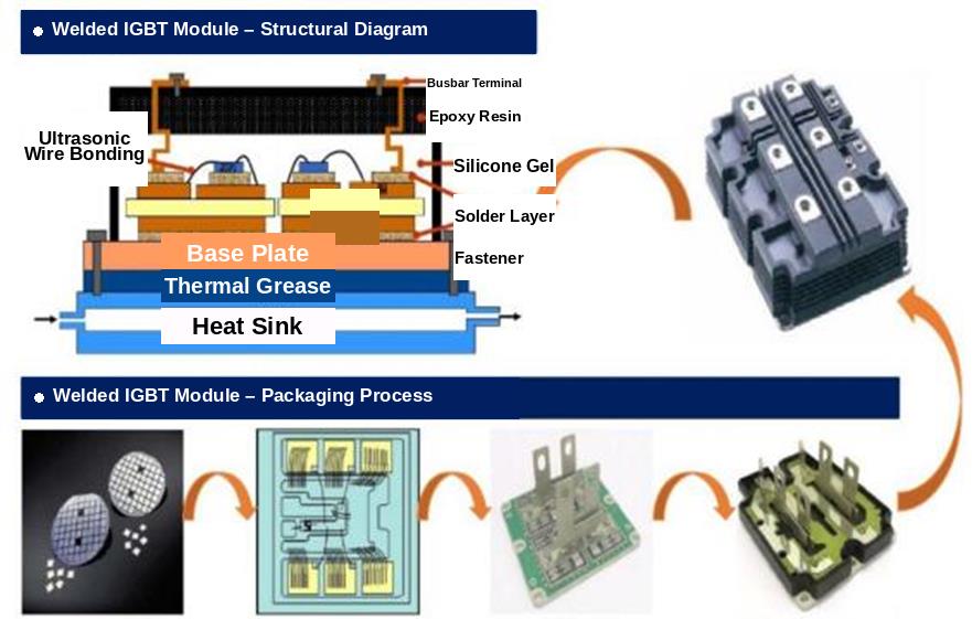
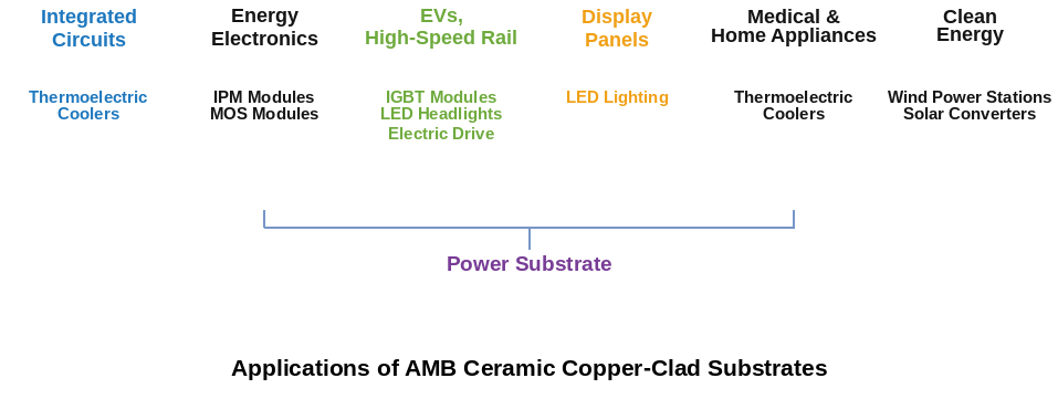
With the rapid development of power electronics technology, the control modules for high-power devices in high-speed rail have created enormous demand for ceramic copper-clad substrates — a key material for IGBT module packaging — with AMB substrates increasingly becoming the mainstream choice.
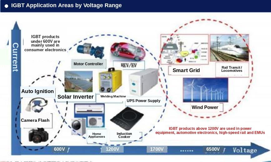
AMB ceramic copper-clad substrates have become the preferred packaging material for new-generation semiconductors (SiC, GaN) and new high-power electronic devices. They are widely used in aerospace and defense, rail traction (such as high-speed rail), power transmission and distribution grids, all-electric ships, electric vehicles, and other applications requiring high-power conversion control and high reliability. AMB ceramic copper-clad substrates are also widely used in ultra-high-power LEDs, semiconductor lasers, thermoelectric coolers, RF and microwave devices, and related fields.
 |
 |
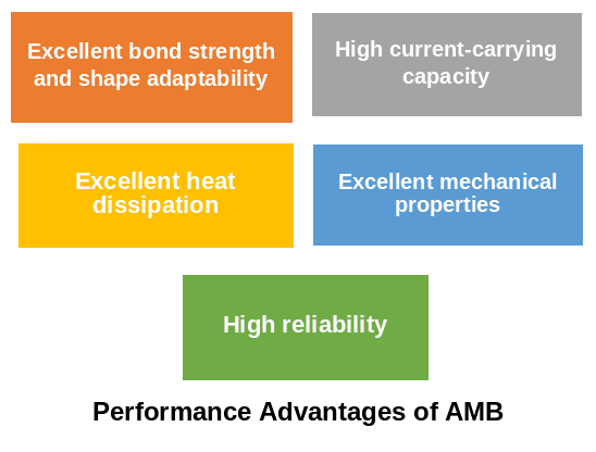
On one hand, AMB substrates offer high thermal conductivity (>90 W/(m·K)), and the thick copper layer (up to 800 µm) also provides high heat capacity and excellent heat transfer.
Therefore, for automotive, wind-turbine, traction, and high-voltage DC transmission applications that demand high reliability, effective heat dissipation, and low partial discharge, AMB silicon nitride substrates are the material of choice.
On the other hand, active metal brazing technology can bond very thick copper (up to 0.8 mm in thickness) onto relatively thin silicon nitride ceramic.
As a result, current-carrying capacity is high and heat transfer performance is excellent. Customers can customize the product layout, similar to a PCB.
 |
 |
| Ceramic Copper-Clad Substrate | Ceramic Circuit Board |
目前,隨著電力電子技術的高速發展,高鐵上的大功率器件控制模組對IGBT模組封裝的關鍵材料——陶瓷覆銅板形成巨大需求,尤其是AMB基板逐漸成為主流應用。